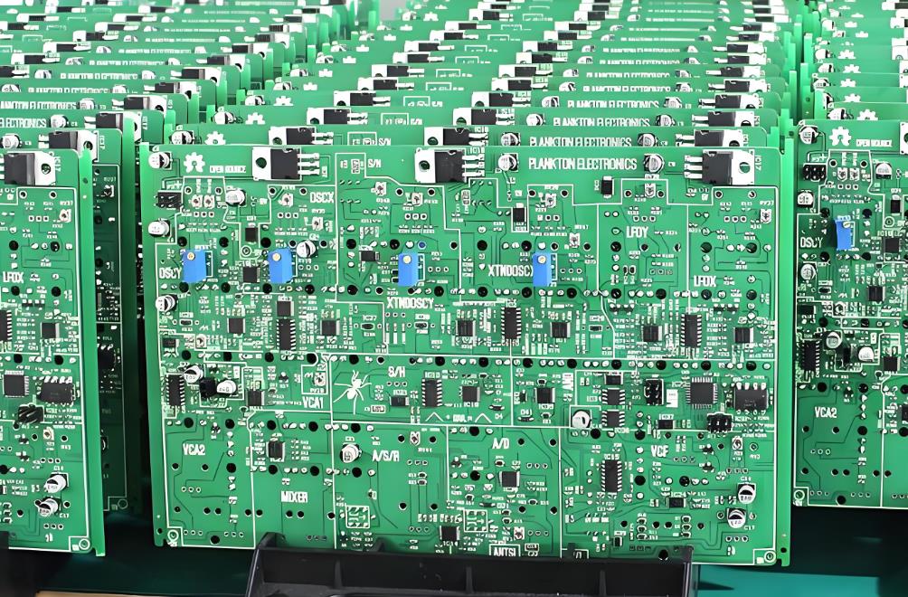
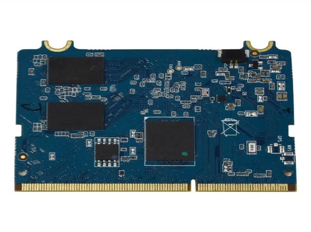
How to Reduce Signal Interference in PCB Design?
In modern electronic devices, signal interference in PCB (Printed Circuit Board) design directly impacts product performance and stability. Minimizing signal interference during the design phase is crucial for improving circuit reliability. Here are some key strategies to achieve this.
1. Optimize Layer Stack-up Design
Multilayer PCBs generally offer better interference resistance than single- or double-layer boards. A well-structured layer stack-up reduces signal coupling and electromagnetic interference. For example, placing signal layers close to ground layers minimizes loop areas and reduces radiation interference. Additionally, using a solid ground or power plane provides a low-impedance return path, further mitigating interference.
2. Keep Traces Short and Straight
Longer traces are more susceptible to interference. Signal traces should be as short and straight as possible, avoiding unnecessary bends. High-speed signals should use differential pair routing and maintain equal trace lengths to reduce common-mode noise. Also, avoid 90° trace bends, as they can cause signal reflection and impedance discontinuity; instead, use rounded or 45° angled traces.
3. Maintain Ground Integrity
Ground design is crucial for interference reduction. A large, continuous ground plane is preferable to single ground traces connecting different circuit modules. When routing high-speed signals, ensure each signal has a dedicated ground reference to prevent excessive loop lengths that could act as antennas and introduce EMI (Electromagnetic Interference).
4. Implement Shielding Techniques
For sensitive signals, consider adding shielding layers or enclosures on the PCB. Using metal enclosures or copper foil around critical circuit areas helps reduce external interference. Grounded copper pours on key signal traces can also minimize electromagnetic radiation.
5. Use Proper Termination Resistors
In high-speed signal transmission, impedance mismatch can cause signal reflections, degrading signal integrity. Adding termination resistors (such as series or parallel resistors) at the end of signal lines helps reduce reflections and improve signal quality. Interfaces like LVDS, USB, and HDMI often require termination to minimize signal interference.
6. Implement Proper Decoupling for Power and Ground
Power noise is a major source of signal interference. Using decoupling capacitors and filter inductors can help stabilize the power supply. Placing decoupling capacitors (e.g., 0.1μF or 10nF ceramic capacitors) close to each IC’s power pins filters out high-frequency noise. Additionally, using power planes instead of individual power traces reduces power impedance and enhances noise immunity.
7. Minimize Loop Areas in Signal Routing
Larger signal loop areas generate more electromagnetic interference. To reduce interference, keep the return path for signals as short as possible. High-speed signals should be routed near ground planes to provide a low-impedance return path. For sensitive signals, using a multilayer design with ground planes shielding the signal layers can effectively reduce interference.
8. Use Filtering Circuits Where Necessary
For low-frequency or DC power noise, LC filter circuits or π-type filters can effectively reduce interference. High-speed digital signals can benefit from ferrite beads or common-mode chokes to suppress EMI. For example, adding an LC filter at the power input can reduce conducted noise and improve circuit stability.
9. Avoid Routing Across Split Planes
In multilayer PCB design, signal traces should not cross split power or ground planes, as this disrupts return paths and degrades signal integrity. All high-speed signals should be routed over a continuous ground or power plane to ensure a smooth return path and minimize interference.
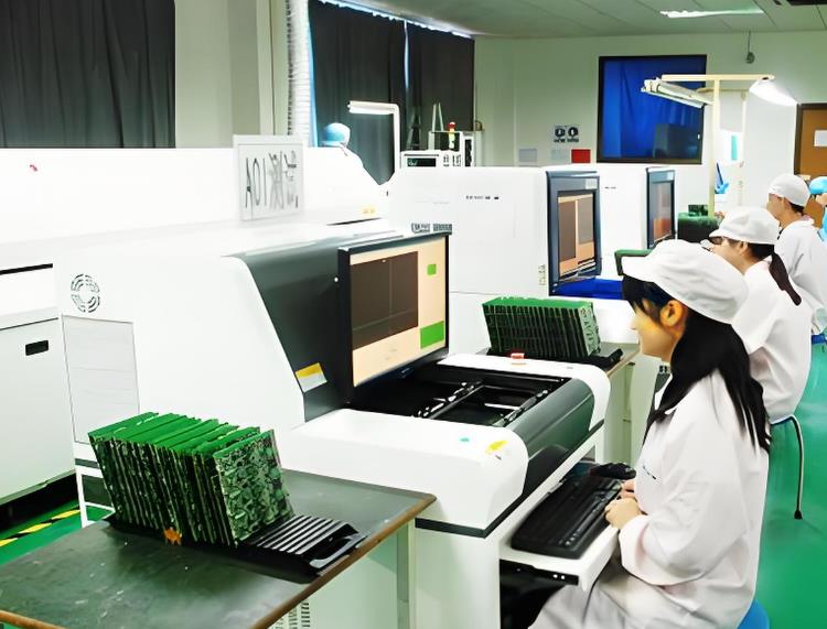
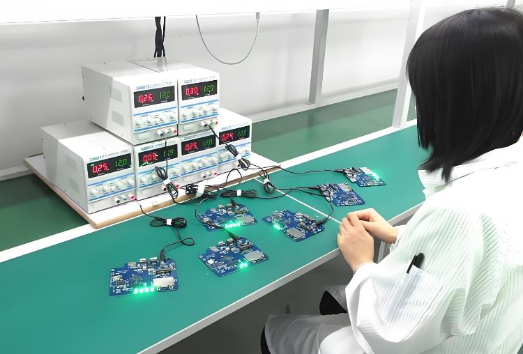
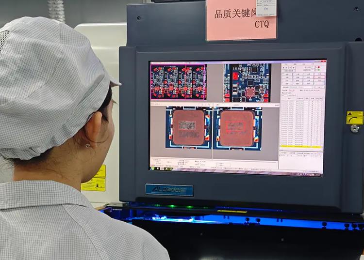
10. Perform Simulation and Testing
After designing the PCB, use signal integrity simulation tools (such as HyperLynx, ADS, or HFSS) for EMC (Electromagnetic Compatibility) analysis to detect potential interference issues. During hardware debugging, tools like oscilloscopes and spectrum analyzers can help measure signal quality and verify that the design meets expected performance standards.
By applying these techniques, signal interference in PCB design can be effectively controlled, improving product reliability and stability. In today’s competitive electronics industry, a well-designed PCB not only reduces interference but also optimizes performance and enhances market competitiveness.
-
-

How to Reduce Signal Interference in PCB Design?
넶6 2025-02-10 -
-
Wave Soldering: Advantages and Disadvantages
넶29 2025-01-06 -
-
How do you handle PCBA?
넶15 2024-12-23 -
-
PCBA Layout vs PCB Layout: Key Differences from Design to Assembly
In the manufacturing of modern electronic products, both PCB (Printed Circuit Board) and PCBA (Printed Circuit Board Assembly) play crucial roles. Within the design process, PCB Layout and PCBA Layout are two important concepts. While they share some similarities, there are significant differences in their applications and importance.
넶10 2024-11-20 -

Exploring the Future: The Innovative Features of Portable Air Pumps!
As technology continues to progress, portable air pumps are rapidly evolving to become smarter, more convenient, and multifunctional. Curious about the surprises that future portable air pumps might bring? Join us on this exciting journey of discovery!
넶14 2024-11-04 -
Exploring Reflow Soldering Technology in SMT Processes and Its Advantages
As market demand for high-quality electronic products continues to grow, the importance of SMT and reflow soldering technologies becomes increasingly prominent. These processes not only enhance production efficiency but also ensure product consistency and reliability. By continually optimizing these workflows, companies can maintain a competitive edge in an intense market landscape.
넶10 2024-11-02