PCBA Layout vs PCB Layout: Key Differences from Design to Assembly
In the manufacturing of modern electronic products, both PCB (Printed Circuit Board) and PCBA (Printed Circuit Board Assembly) play crucial roles. Within the design process, PCB Layout and PCBA Layout are two important concepts. While they share some similarities, there are significant differences in their applications and importance.
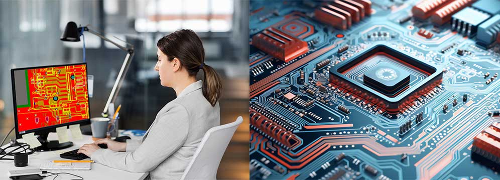
What is PCB Layout?
PCB Layout refers to the process of designing the electrical connections and routing of components on a printed circuit board. This process typically involves the arrangement of electrical circuits, trace routing, and pad placement to ensure the functionality and manufacturability of the PCB. The main goal of PCB Layout is to ensure the smooth flow of signals, proper connections between components, and adherence to manufacturing standards, so that the board operates efficiently and reliably.
What is PCBA Layout?
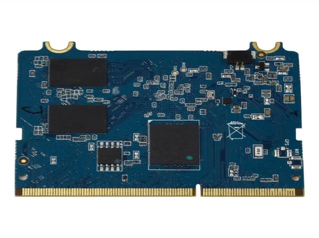
PCBA Layout, on the other hand, goes beyond PCB Layout by focusing on the actual placement of electronic components on the PCB and their electrical connections. Unlike PCB Layout, PCBA Layout takes into account the size, package types, and installation orientation of components, along with considerations for assembly processes. In other words, while PCB Layout serves as the design blueprint, PCBA Layout provides a detailed guide for the assembly process, directly influencing production efficiency, stability, and product performance.
Key Differences Between PCB Layout and PCBA Layout
1. Design Scope
·PCB Layout focuses on the basic structure and electrical connections of the circuit, dealing with how to route the traces, connect the components, and ensure signal integrity. It addresses the fundamental problems of electrical connection and circuit design.
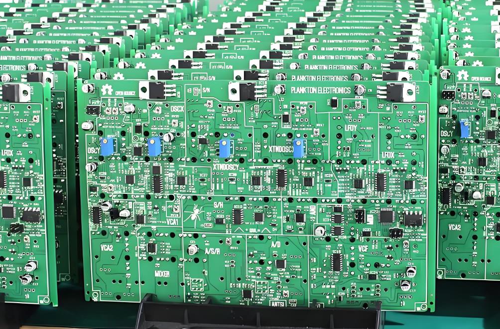
·PCBA Layout builds on the PCB Layout by considering where each component will be physically placed on the board, its size, orientation, and how these components will be assembled in the manufacturing process. It’s a more detailed, assembly-oriented design that aims to optimize the final product assembly.
2. Focus Areas
·PCB Layout primarily addresses electrical performance, signal integrity, and the overall functionality of the circuit board.
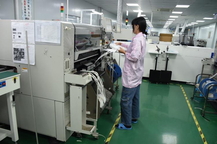
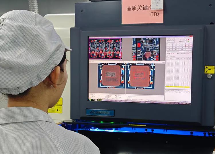
· PCBA Layout, however, is more concerned with manufacturing feasibility, component placement, thermal management, and assembly efficiency. It considers factors such as component spacing, layout for SMT (Surface Mount Technology), heat dissipation, and more.
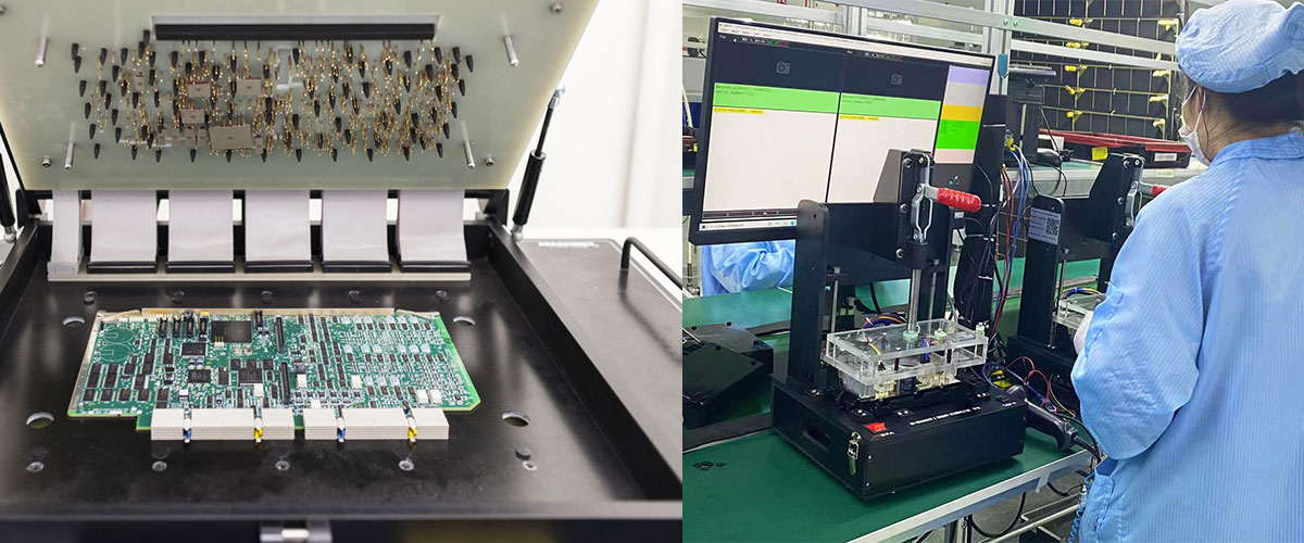
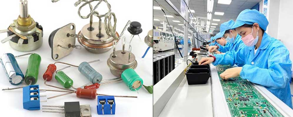
3. Manufacturing and Assembly Differencs
·Once PCB Layout is completed, it is passed to a PCB manufacturing facility to create the bare board.
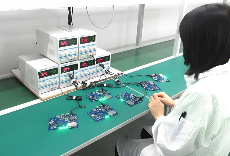
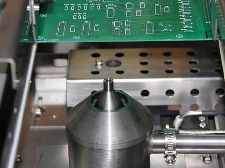
· PCBA Layout, however, deals with the next stage of production: the actual placement and soldering of components onto the PCB. This process involves ensuring that components are correctly positioned for automated assembly and that the design adheres to the production line’s capabilities.
Why is PCBA Layout More Important?
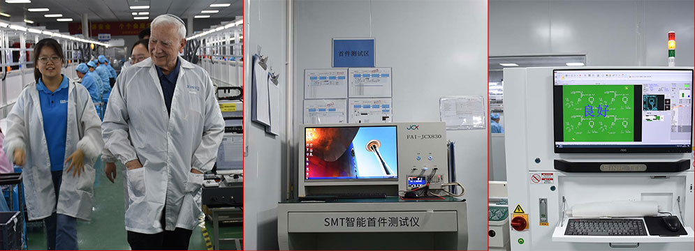
While PCB Layout is the foundation for the electrical design of a circuit board, PCBA Layout plays a pivotal role in determining the final product's quality and manufacturing efficiency. A well-optimized PCBA Layout can greatly enhance assembly line productivity by minimizing errors and maximizing precision. It ensures that components are placed in a way that reduces thermal and electrical issues, making the final product more reliable and efficient. In large-scale production, an optimized PCBA Layout reduces rework, minimizes waste, and lowers production costs, ultimately improving product consistency and reliability.
Conclusion
PCB Layout and PCBA Layout are two interconnected phases in the design of electronic products. While PCB Layout addresses the electrical design, PCBA Layout ensures the board’s assembly and performance in the real world. Both are essential, but PCBA Layout takes on greater importance when it comes to manufacturing and assembly efficiency. For engineers, understanding the distinctions between these two aspects and ensuring that both the circuit design and the assembly process are properly optimized is key to success. In today’s competitive electronics market, having a carefully designed PCBA Layout is undoubtedly a significant advantage for any business.
-
-
How to Reduce Signal Interference in PCB Design?
넶6 2025-02-10 -
-
Wave Soldering: Advantages and Disadvantages
넶29 2025-01-06 -
-
How do you handle PCBA?
넶15 2024-12-23 -
-

PCBA Layout vs PCB Layout: Key Differences from Design to Assembly
In the manufacturing of modern electronic products, both PCB (Printed Circuit Board) and PCBA (Printed Circuit Board Assembly) play crucial roles. Within the design process, PCB Layout and PCBA Layout are two important concepts. While they share some similarities, there are significant differences in their applications and importance.
넶10 2024-11-20 -

Exploring the Future: The Innovative Features of Portable Air Pumps!
As technology continues to progress, portable air pumps are rapidly evolving to become smarter, more convenient, and multifunctional. Curious about the surprises that future portable air pumps might bring? Join us on this exciting journey of discovery!
넶14 2024-11-04 -
Exploring Reflow Soldering Technology in SMT Processes and Its Advantages
As market demand for high-quality electronic products continues to grow, the importance of SMT and reflow soldering technologies becomes increasingly prominent. These processes not only enhance production efficiency but also ensure product consistency and reliability. By continually optimizing these workflows, companies can maintain a competitive edge in an intense market landscape.
넶10 2024-11-02